CT Scanning for IC Inspection
In the semiconductor and electronics industries, X-ray imaging is widely used to inspect internal structures and defects. This includes checking manufacturing tolerances, assembly errors, and packaging defects in final products, as well as quality control in individual processes such as post-SMT inspections for cold solder joints, voids, and solder bridges, and single-chip packaging checks. Advanced inspections, such as wafer analysis, multilayer PCB via quality assessments, and stacked packaging evaluations, are also prevalent. X-ray imaging is essential for both root cause analysis in laboratories and real-time quality control on production lines.
Applications of X-ray Imaging in Printed Circuit Boards
On production lines, AOI and 2D X-ray imaging complement each other. Visible light AOI is used to detect surface damage and defects from the printing process, while 2D X-ray imaging reveals manufacturing defects hidden under packaging structures. As the inspected structures grow more complex, such as with multilayer PCBs, 2.5D/3D stacking (CoWoS), and Fan-Out Panel-Level Packaging (FOPLP), traditional 2D X-ray imaging faces challenges. It struggles with stereological errors from overlapping structures, making it difficult to accurately locate defects and perform tasks like quantification and geometric measurements.
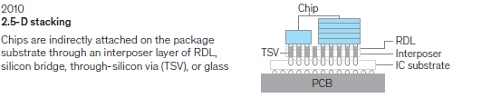
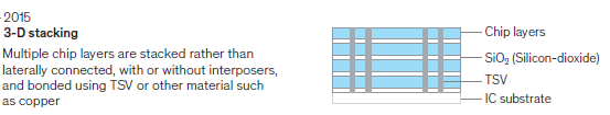
Different Types of Stacked Packaging 1
To characterize defects in complex structures, support Failure Analysis (FA), and help production units identify process defect causes, laboratories often use High-Resolution MicroXCT systems for non-destructive imaging. A commonly used imaging and reconstruction method is Circular-based Computed Tomography (CBCT). This cone-beam CT technique is ideal for inspecting small-scale three-dimensional samples and reconstructing internal structures at the micron level.
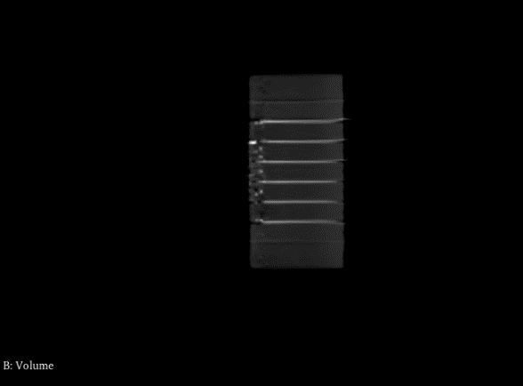
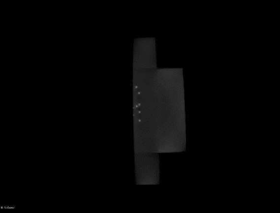
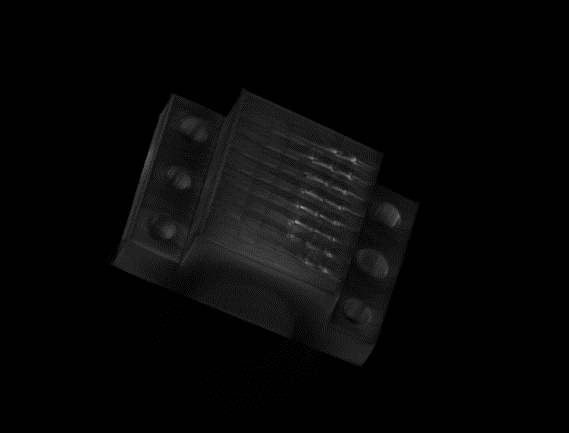
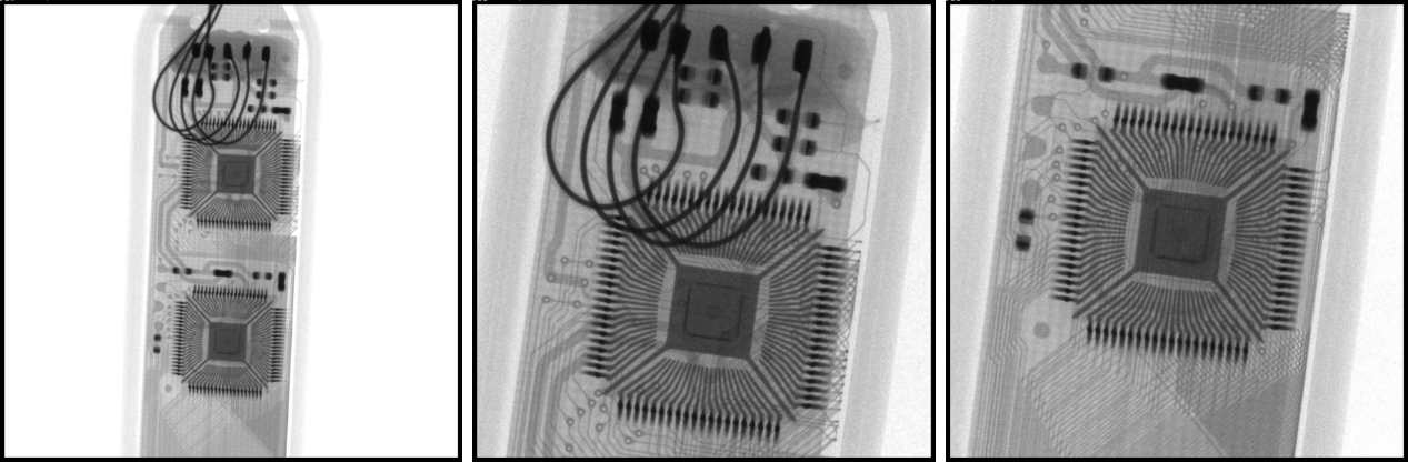
CT Images of Circuit Fixtures for IC Inspection
In the semiconductor and electronics industries, the objects inspected are often flat samples, such as circuit boards, packaged integrated circuits, and wafer materials. To obtain the required geometric projection space for Circular-based Computed Tomography (CBCT), these samples must be clamped and fixed vertically. However, clamping and rotating delicate samples in this orientation presents risks and challenges. Moreover, because flat samples have a disproportionate thickness-to-length ratio, rotating them to certain angles can cause excessive contrast. This results in insufficient sampling rates and a higher likelihood of artifacts in the reconstructed images.
To address this issue, advanced imaging systems use Computed Laminography (CL), which allows the sample to rotate horizontally on a platform. This approach mitigates challenges related to gravity and enables the selective magnification and observation of specific areas, known as the Region of Interest (ROI). In CL imaging, clear images are focused on a particular height and area, but structures outside the ROI may experience significant reconstruction artifacts. A similar strategy is used in Partial Angle Vertical CT, which employs localized angle imaging to enhance resolution in vertical structures, though it demands even greater precision in mechanical movements.
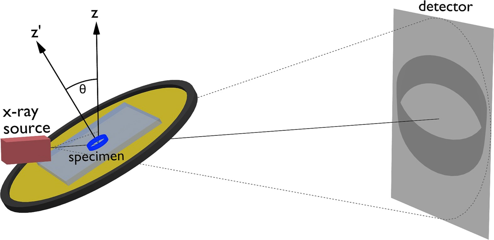
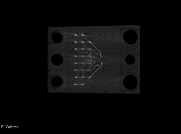
Spatial Geometry of Computed Laminography
However, both CBCT and CL methods currently only offer offline inspection solutions. While laboratory machines achieve high precision and excellent image quality, they do not meet the throughput demands of production lines. To address this, both efficiency and process flow designs must be faster, more advanced, and capable of keeping up with production line speeds.
Recently, mainstream solutions have used angled perspective imaging to produce 2.5D image stacks for defect detection and allocation through image analysis. While this method reduces imaging time, it does not overcome the fundamental limitations of perspective imaging in depth perception, leading to issues with insufficient information and potential misinterpretation. This approach only partially addresses production line needs for specific applications. True 3D imaging is necessary to accurately detect small defects in complex structures. With Induxray’s technology in innovative In-Line CT, combined with Sparse-Projection Reconstruction algorithms, brings advanced 3D imaging capabilities from the lab to the production line. This solution meets the demand for rapid inspection and is ideal for comprehensive inspection of sophisticated product lines.
1 P25, Exhibit 1, Timeline of packaging technology Packaging technology for semiconductors has evolved quickly since 2000, McKinsey on Semiconductors, Number 9, March 2024.