Copper Clad Laminate (CCL) Inspection
Copper Clad Laminate (CCL) is a key upstream material for PCBs and is widely used in communication systems, consumer electronics, transportation and power systems, as well as in the continuous upgrades of high frequency and high speed networking equipment. The global CCL market currently has an annual production value of approximately USD 16.4–18.8 billion (2023–2025), with a CAGR of 5.6–6.1%1. Recent market assessments indicate that growth momentum will come from demand in 5G infrastructure, AI servers, and intelligent charging/discharging devices.
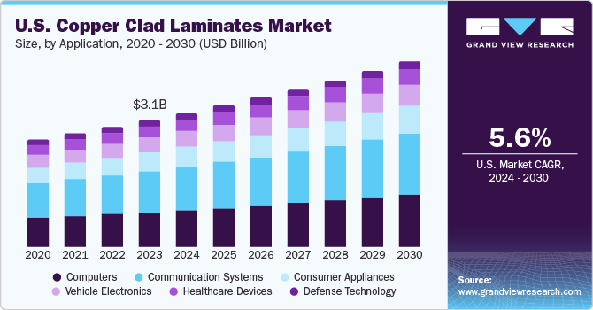
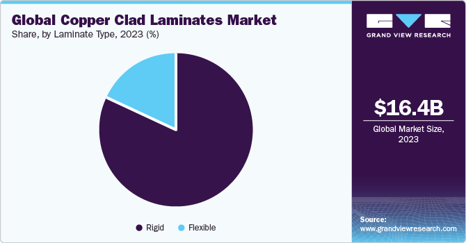
Figure 1. CCL Market Trends and Global Market Share
The structure of CCL consists of copper foil (conductive layer) bonded with dielectric substrate/reinforcement materials (glass fiber fabric, non woven fabric, or paper), laminated with resin systems (epoxy, phenolic, PI, PTFE). CCL can be single sided, double sided, or multilayer. Copper foil types include Electro Deposited (ED, used for rigid boards) and Rolled Annealed (RA, used for flexible and bending required applications). Dielectric and reinforcement materials range from FR 4 resin (general use), glass fiber with high Tg and low Dk/Df (for high speed/high frequency applications), to PI/ceramic/PTFE (for high temperature or RF applications). In some cases, metal core or composite substrates are used to address high power and thermal management challenges.
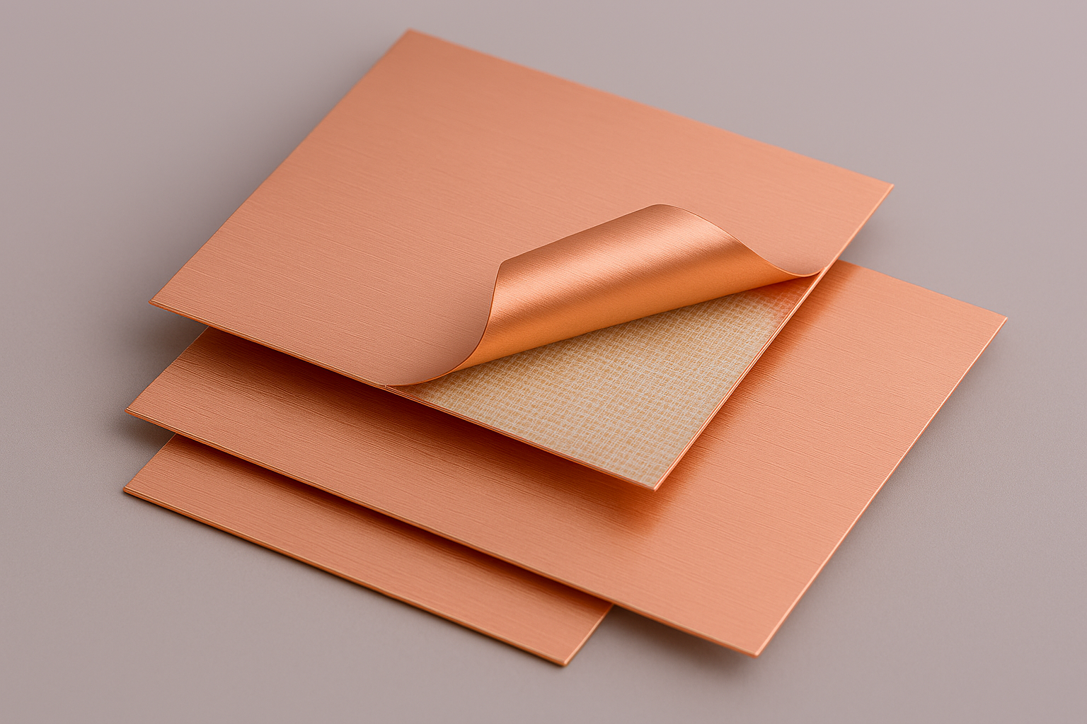
Figure 2. Illustration of CCL Materials
In the past, AOI inspection has been used mainly to identify visible light defects such as copper missing, scratches, or contamination on the surface. However, defects within the substrate such as voids, cracks, structural warpage, delamination, and thickness/density variations caused by materials or processes can only be detected through X ray imaging. The samples used in this study are double sided copper coated non woven substrates. X ray imaging is used to detect covered scratches as well as internal defects such as delamination, uneven density, and thickness variation.
We employed a high resolution X ray source, adjusted magnification and acquisition parameters, and used image processing techniques to enhance the copper foil and non woven contrast. Scratches on the non woven fabric were created with a tool (width ≈ 0.5 mm, length ≈ 15 mm, depth ≈ 0.1 mm), and then we compared X ray images of areas with and without copper foil coverage. In addition to visual analysis, pixel absorption values along specified paths were extracted to generate pixel distribution curves, allowing evaluation of thickness and density variations.
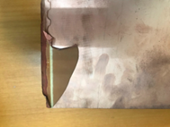
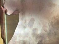
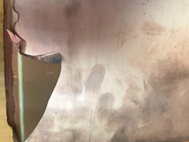
Figure 3. Original CCL Sample, Scratch Location, and Visible Light Comparison When Covered by Copper Foil
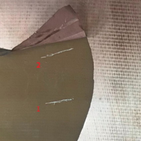
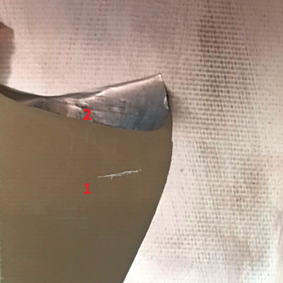
Figure 4. Enlarged Visible Light Comparison of Scratch Location With and Without Copper Coverage
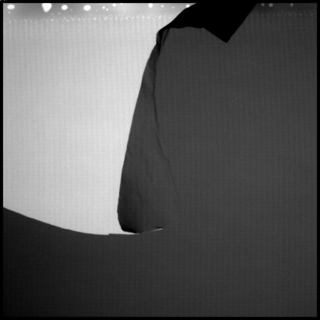
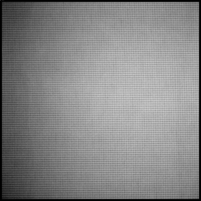
Figure 5. X ray Images of Scratch Location vs. Normal Substrate Area
X ray images clearly reveal the texture of the non woven fabric and the structure of double layer copper foil. In both simulated single layer and double layer copper conditions, creases, scratches, and internal substrate structures remain distinctly visible under X ray. Below are enlarged regions showing the scratch both exposed on a single copper layer and covered under dual copper layers, with the scratch locations marked.
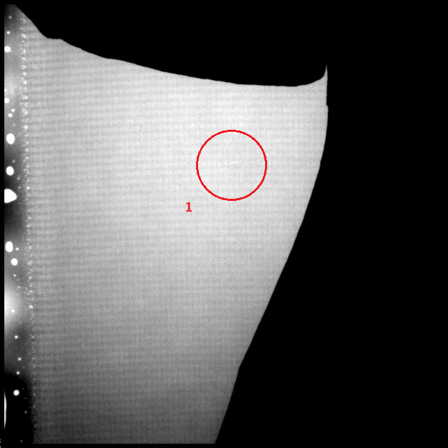
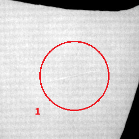
Figure 6. X ray Image of Scratch on Single Layer Copper (Uncovered) and Enlarged View
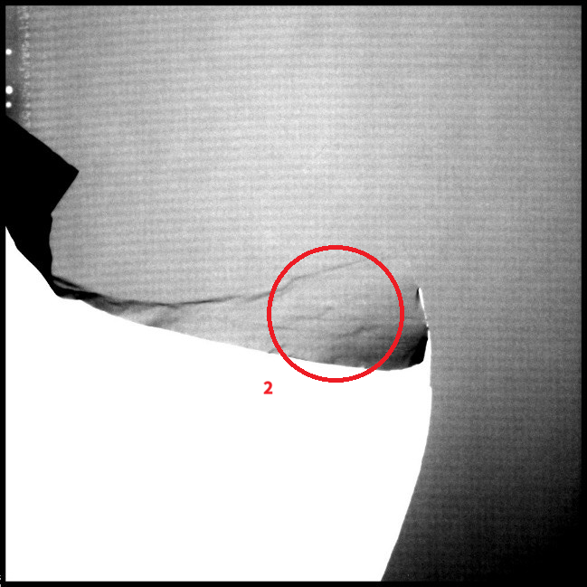
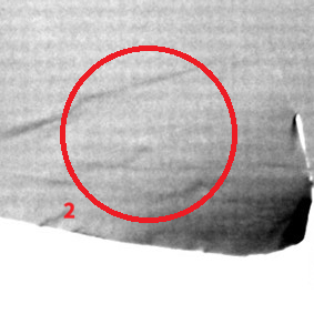
Figure 7. X ray Image of Scratch Under Dual Layer Copper Coverage and Enlarged View
For quantitative analysis, pixel absorption (grayscale) along selected paths is extracted to build position absorption curves. By examining slopes and peak valley patterns, we quantify thickness/density trends and can further define Δ absorption thresholds and coefficients of variation as process control indicators. Significant thickness variation in the material is clearly observable.
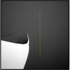
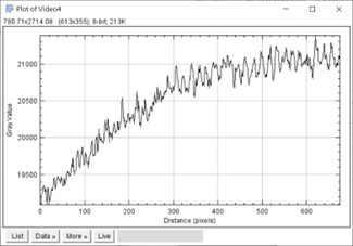
Figure 8. Pixel Value Analysis and Distribution Curve Along Sampling Path
Future product inspection especially real time in line quality control will rely on AOI + AXI integration: AOI for high speed surface screening, and AXI to detect internal structural defects. Combined assessment improves yield. For large raw material substrates, such as 500 mm (L) × 500 mm (W) × 1 mm (T), high resolution imaging and multi point continuous scanning enable full production line inspection.
Induxray’s PortalX imaging platform provides real time dynamic imaging to support in line inspection. Its modular and highly customizable architecture allows seamless integration with customers’ automation equipment and production lines, while also supporting the deployment of intelligent algorithms and Statistical Process Control. By establishing pixel to physical measurement mapping models, PortalX can output thickness trends, density variation indicators, void ratio, and more. It can also integrate with Manufacturing Execution Systems (MES) to trace inspection results alongside batch information, recipes, and machine data, enabling comprehensive archiving of images and analysis results and providing complete data for downstream Failure Analysis (FA).
1 Copper Clad Laminates Market (2024 - 2030)
https://www.grandviewresearch.com/industry-analysis/copper-clad-laminates-market-report